


Gallium Nitrate (GaN) is a rigid, mechanically stable and wide bandwidth semiconductor material. It can transmit higher voltages and performs better than silicon-based devices. This is thanks to the fact that GaN has a faster switching speed, high thermal conductivity and lower resistivity. GaN technology is used in the manufacturing of semiconductor power devices (such as charging machines), RF components and LED lights.
Gallium Nitrate crystals can be enlarged on various substrates, such as Sapphire and Silicon Carbide (SiC). When the GaN epi layer is enlarged on silicon, it reduces the costly special manufacturing requirements and makes it possible to benefit from the silicon sheets that can be supplied at a low cost. This reduces the manufacturing costs of GaN technology.
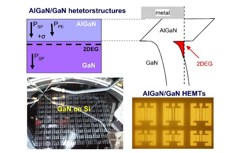
Although the manufacturing cost of GaN devices is higher than silicon-based devices, it is lower than that of MOSFET devices. This is because GaN devices can be manufactured at factories that manufacture silicon semiconductors without deviating from standard silicon manufacturing processes. Although these devices are small, their functional performance is pretty higher.
History of Gallium Nitrate (GaN):

Gallium was first discovered as a semiconductor in 1875 by the French scientist Paul Emile Lecoq de Boisbaudran. This discovery filled the gap in Mendeleev’s periodic table. Gallium nitrate (GaN), on the other hand, was obtained in 1938 by passing ammonia over the hot gallium element and crystallizing it on a small scale.
GaN initially started to be used in the LED field. Afterwards, it gained a great importance after an electron velocity test conducted at the United States Army Research Laboratory in 1999. This test revealed that the electrons move at a very high speed (1500 cm2/(V·s) at 300 K) in GaN.
The first GaN materials started to be introduced in 2006 as GaN HEMT (High Electron Mobility Transistors). Since 2008, they have been available as MOSFETs as we currently name them.
The silicon, SiC and GaN material properties comparison table is shown below.
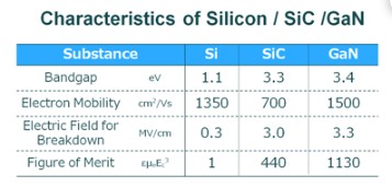
Looking at the above table, it can be assumed that GaN does not have a big difference than SiC in terms of bandwidth and electrical breaking strength. However, the most important feature that distinguishes GaN from other materials is its electron transport capacity at high speeds. This means that the element can be opened and closed at a very high speed.
How is Gallium Nitrate (GaN) Used in Semiconductor Technology?
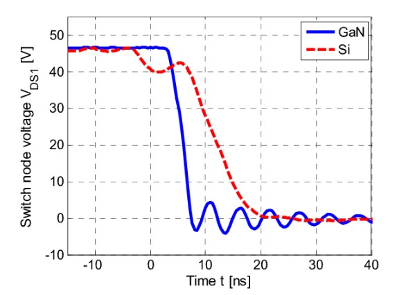
In the example above, the closing speeds of classical Si and GaN MOSFETs with the same voltage, current and internal resistance values are shown. This important difference allows the circuits to operate at much higher frequencies, especially as it significantly reduces switching losses. This makes GaN a preferred element in high-frequency applications, although its other properties are similar to SIC. The reason why it is so popular particularly in the military field, is that it can be used in systems that require high power, such as radars.
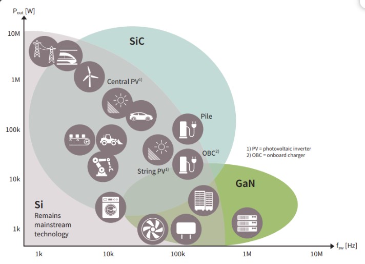
Although GaN is a suitable element for fast switching, it is necessary to change the mechanical connection structures due to reasons such as stray inductance and parasitic capacities that affect fast switching and lead to limited power values. Moreover, in order to highlight the high switching characteristics, the upper limit of the voltage values is around 900V. Due to this limitation, GaN lags behind Si and SiC devices in high-power applications, as can be seen in the above table.
What Are the Benefits of Gallium Nitrate (GaN)?
- High Electron Mobility:
Efficient Performance: GaN provides higher switching speeds and lower energy loss due to its high electron mobility. This is especially essential in high-frequency and high-power applications. - Wide Bandwidth:
Higher Energy Efficiency: The wide bandwidth (3.4 eV) of GAN allows it to operate at higher efficiency. This offers a huge advantage, especially in optoelectronic devices such as LEDs and laser diodes.
High Temperature Stability: The wide bandwidth allows GAN to work stably at high temperatures, which makes it ideal for high temperature applications. - High Power Density:
Smaller and Lighter Designs: GaN devices allow for smaller and lighter designs with their high power density. This is particularly advantageous for mobile electronic devices and electric vehicles. - High Thermal Conductivity:
Effective Heat Management: The high thermal conductivity of GAN provides better heat management. This allows the devices to work with higher efficiency and for a longer time. - High Frequency Performance:
Telecommunication and Radio Frequency Applications: GaN is ideal for high frequency applications. It is widely used in telecommunication, radio transmitters and microwave devices. - Energy Efficiency:
Less Energy Consumption: GaN-based devices consume less energy than silicon-based devices. This translates into energy savings and lower operating costs. - High Temperature Resistance:
Reliability: GaN can work stably at high temperatures. This ensures reliable performance in harsh environmental conditions. - Longer Service Life:
Durability: GaN devices are long-lasting and durable. This reduces maintenance costs and ensures long-term reliability. - Optoelectronic Advantages:
Bright and Efficient LEDs: GaN is used in the manufacturing of blue and green LEDs and provides high brightness and efficiency.
High Performance Laser Diodes: GaN laser diodes offer high efficiency and durability, which is essential in optical data transmission and optical storage devices.

With the introduction of new materials in semiconductor technology, in the future we will use different types of materials in various applications such as high frequency, high power and high voltage. GaN has been recognized by designers, particularly in the industries with high power density, such as telecommunications and military field. Manufacturers have begun to improve the GaN products that have a complex gate sliding part. These improvements indicate that GAN will become a major player in electronics industry in the coming years. These benefits offered by GAN make it an indispensable material in modern electronics, optoelectronics, telecommunications and power electronics applications.