


PCB Production Stages


ELECTRONIC BOARDS MANAGER
Design and Import of Gerber File
Drawings are made with PCB drawing software and files are prepared in the format desired by the manufacturers. The most common of these is the Gerber format.
Pre-Manufacturing Engineering
The data provided by various software (Gerber and Hole files) are used to produce the manufacturing files. Engineers compare the suitability of the board for production according to production standards.
Cutting of Copper Plates to be Used in Production
The raw material to be used in production is prepared by cutting the plates, but cleaning should be given a huge importance in this process. Dirt or a stain may cause short or open circuits.
PLOTTER- Getting a Movie Output
After checking the suitability of the board for production, a film printout of the board is taken with a special printer. These printers use highly sensitive printing technology to provide a detailed film of the design. Black ink shows the conductive areas of the PCB. The remaining areas are the insulating parts.
The solderable area on the” PCB” should be smooth and flat.
Printing of the Film on the Copper Plate
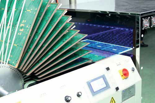
The extracted film is a photosensitive dry film and is transferred to the copper material using UV light. This process is performed in a clean area free from dust. There are multiple methods for printing the film.
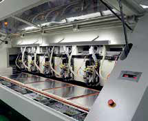
ETCHING Process (Etching of Copper)
It is the removal of unwanted copper using a strong alkaline solution. During etching, the PCB boards are lowered into an acid pool and removed after a certain time.
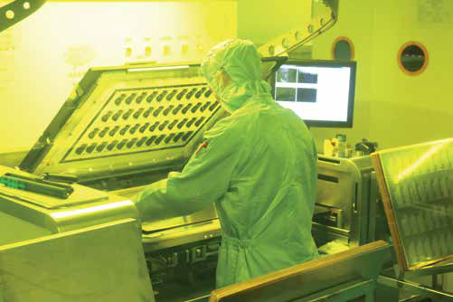
Drilling of Holes and CNC
At this stage, drilling process is started by determining the necessary references with hole drilling machines. Air-pressure drill bits are used in the drilling process, which rotate at about 150,000 rpm.
Soldermask Application (Solder Mask)
The next step after punching is to cover the board with a solder mask. The solder mask can be in different colors. Usually green is used.
Material Printing (SilkScreen)
It is the process of printing the necessary letters and electronic component references on a PCB board.
Surface Finish (Solder Coating)
In order to ensure the solderability of the PCB board, the PCB boards are dipped into a solder pool and removed as “paneled” or “single”.
● The solderable area should be smooth and flat.
● The main types of coating are as follows.
● Solder coating (leaded or lead-free), nickel and gold plating and organic plating (OSP)
V-CUT and ROUT Process
SMD is the process, by which the paneled boards are separated from each other and the internal and external cutting processes of the produced boards are applied in order to facilitate compliance with the placement and production stages.
Electrical Testing
● Each board is electrically tested according to the original file.
● Whether the paths are short-circuited or open-circuited, as well as their compliance with the original file is tested.
● There are two types, made through “fly probe” and “test fixture”.
● Fly probe is mainly used in sample production.
● E-test fixture is used in mass production and is a fast testing method.