


PCB ELECTRONIC CARD MANAGER
In order your PCBs to be produced without any issues, it must be compatible with the machine capabilities and production processes in your production facilities. These factors may vary depending on the characteristics of the equipment, machinery and PCB, as well as the situations in which the CAD/CAM engineer who prepares the production file can take initiative. The common goal is to ensure PCB availability and prevent the predicted PCB production problems. What we will discuss in this article is not about controlling production capacity such as the distance between paths, minimum paths and “via diameters” in the design, but rather about some changes that need to be made in your existing design for smooth and accurate PCB production. Now, let’s examine such situations with some examples and pictures.
Necessary changes made for the holes:
0.15 mm is added to the coated (PTH) hole diameter to provide your final hole dimensions in your design. It is usually 0.10 mm in gold plating. The uncoated (NPTH) is 0.05 mm. Special attention should be paid to this situation in your Via designs, the wall thickness of the hole and copper ring should be left at a minimum of 0.3~0.4 mm (total) copper. This change is made by the PCB manufacturer’s engineer, and if there is not enough space, the final hole dimensions will remain small. Usually, a drilling bit is used for holes of up to 6 mm, while CNC is used for larger ones, and its tolerance is ±0.1 mm. It is also recommended that the safety margin around it be 0.25 mm.
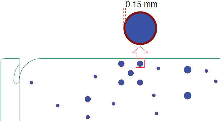
Example 1: Comparison of the drill layer (blue) of the original Gerber and that of the manufacturer’s Gerber (red)
Note: 0.15mm has been added to the coated (PTH) hole diameter of the production Gerber.
“As Ozdisan Elektronik PCB department, we share the changes to be made in customer’s Gerber with the customer along with engineering questions, in order to get approval and apply the related changes.”
Necessary changes made to the Gerber for the silkscreen process:
In some data, references can remain above the surface that can be soldered. In this case, the parts of the lettering should either be deleted or moved to a suitable place. Otherwise, it prevents the pad from getting soldered in a post-surface coating process since the silkscreen is also a paint. In some designs, when the lettering is below the production limits in terms of thickness and height, it must be deleted or increased in size.
Example 2a: Comparison of the original Gerber soldermask layer (red) with the silkscreen layer (blue)
Example 2b: Comparison of the original Gerber silkscreen layer (blue) with the production Gerber silkscreen layer (green)
Note: Since the silkscreen layer in the original Gerber overlays on the surface that received the solder, there was trimming and transport on the silkscreen in the production Gerber.
Necessary changes made to the Gerber for the V-CUT and CNC process:
Firstly, the V-CUT operation does not change the board size. Therefore, in some original Gerbers with panels, a distance of 0.5-1 mm can be left between the boards. In such a case, information is required. The outer cut of the board will increase by 0.5 mm -1 mm, or it is recommended to remove the clearance between the boards. The outer cut safety margin is 0.4 mm. If the distance between the outer cut and the copper path on the V-CUT path is less than 0.4 mm, the copper path must be moved or the copper must be clipped so that the distance remains 0.4 mm. Otherwise, it will stay here and a burr will form. This results in a risk of creating short-circuit problems, which is unclear when to occur. The outer cutting safety margin for CNC machining is 0.25mm.
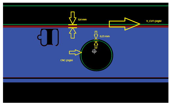
Example 3: Comparison of the copper layer of the original Gerber (red) with the copper layer of the production Gerber (blue)
Note: The clearance between the copper layer and the outer cutting line is 0.4mm for V_cut and 0.25 mm for CNC cutting.
Example 4: Comparison of the soldermask layer of the original Gerber (red) with the copper layer of the production Gerber (blue)
Note: The soldermask layer of the production Gerber has been enlarged to be more than 3 shafts larger than the size of the copper data.
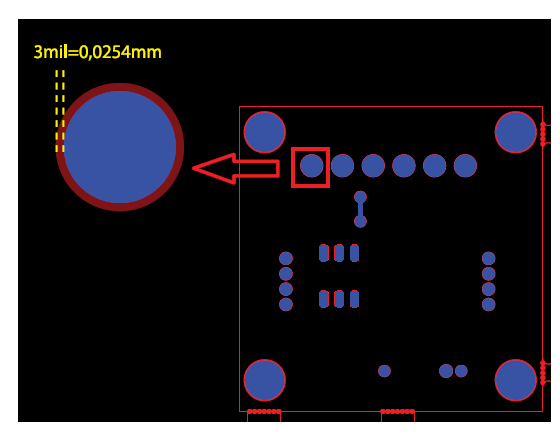
Necessary changes made to the Gerber for the soldermask process:
This process depends on the sensitivity of the method used by the manufacturer in the soldermask process. The soldermask should be 3 shafts larger (from all sides). The reason is to ensure that the film data used in the processes overlap. The purpose is to keep the solderable area stable. Otherwise, the surface that will receive solder will shrink, and difficulties may occur in soldering operations.
The PCB department at Ozdisan Elektronik shares the changes to be made in customer Gerbers with the customer through engineering questions, gets approval and makes the necessary changes. Ozdisan’s goal here is to produce the closest version to the customer’s production Gerber, without any errors.