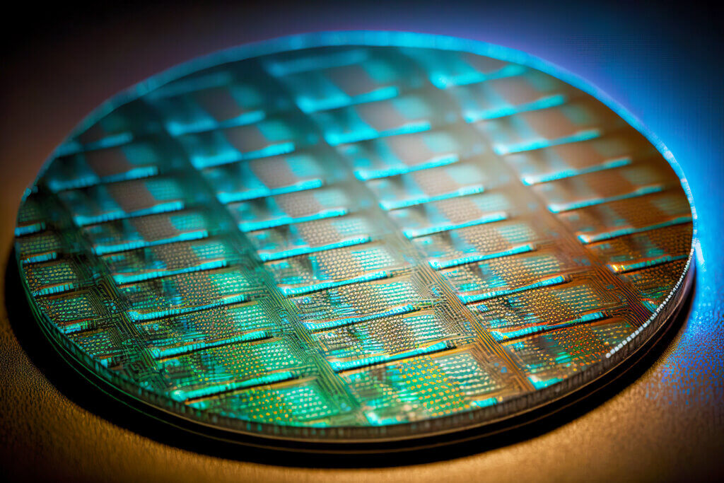

Wafer is an essential material used in the manufacture of semi-conductor circuit elements, solar cells and integrated circuits. Wafers, which are in the form of a thin disc, are usually manufactured from silicon raw material.
The manufacturing of wafer requires advanced technology and must meet some international standards. Countries such as China, USA, Japan, South Korea, Taiwan are the leading countries in wafer manufacture in the world.
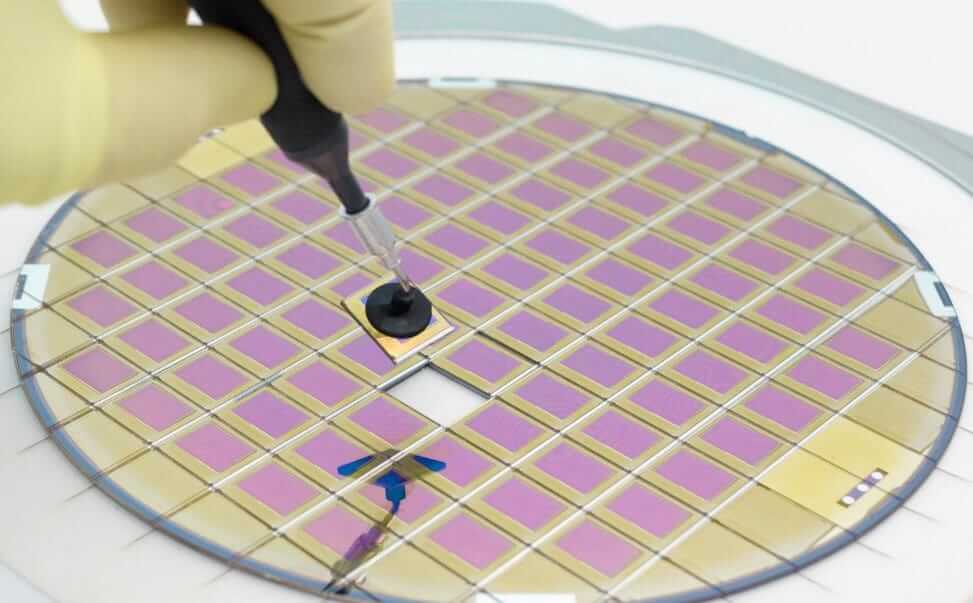
How is Wafer Manufactured?

Wafer manufacturing, consisting of many different stages, includes the following processes (respectively);
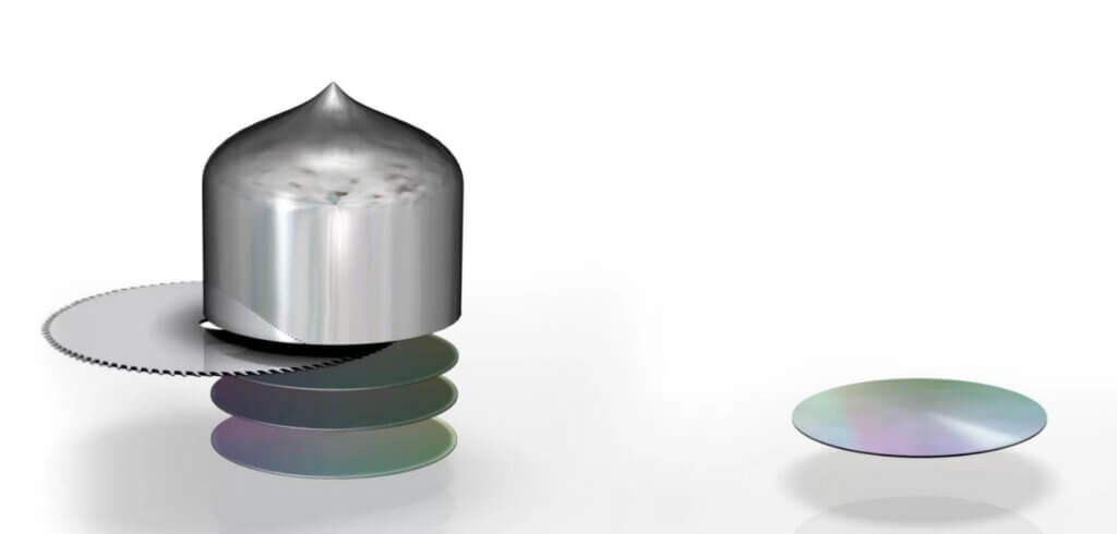
1. Silicon Crystal Growing: Silicon crystals are obtained from high-purity silicon sources and grown under high temperature and pressure in special furnaces.

2. Silicon Cutting: The grown silicon crystals are cut into thin slices, and wafers are obtained.
3. Silicon Processing: Wafers are subjected to chemical treatments to smooth and clean their surfaces.

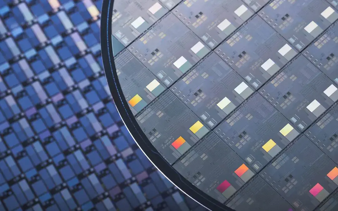
5. Testing and Cutting: The integrated circuits on each wafer are tested and then cut off to obtain individual integrated circuit chips.
What are the Standards in Wafer Sizes?
Wafer manufacturing diameters vary according to the requirements of technology and are usually available in the following standard sizes.
- 2 inches (50.8mm): These are usually used in research and development applications.
- 4 inches (101.6 mm): They are widely used in semiconductor manufacturing.
- 6 inches (152.4 mm): This is the industry standard and used in most integrated circuit manufacturing.
- 8 inches (203.2 mm): They are used in large-scale semiconductor manufacturing.
- 12 inches (304.8 mm): They are used for high-performance processors and memory chips.
- 18 inches (450mm): They are newer and in larger sizes. They have not yet become an industry standard, but may offer the potential for more chip manufacture in the future.
These diameters represent the wafer sizes used in various applications such as microchip manufacturing and solar panels. In particular, larger diameter wafers allow for manufacturing of a larger number of chips, which increases cost-effectiveness.
What are the Areas of Use of Wafer?

Wafers are used in many different areas in the electronics industry. They are fundamental components, especially in the manufacture of integrated circuits, microchips, sensors and other semiconductor devices.
Many integrated circuits used in computers, mobile phones, medical devices, automotive systems, communication equipment and several other technological devices are built on wafers.
Wafer technology forms the basis of the microelectronics industry and accommodates a wide range of technologies.
These include CMOS (Complementary Metal-Oxide-Semiconductor), BiCMOS (Bipolar-CM Dec), BJT (Bipolar Junction Transistor), MOSFET (Metal-Oxide-Semiconductor Field-Effect Transistor) and some others. These technologies are used in the design and manufacture of integrated circuits for different applications.