


ELECTRONIC BOARDS RESPONSIBLE
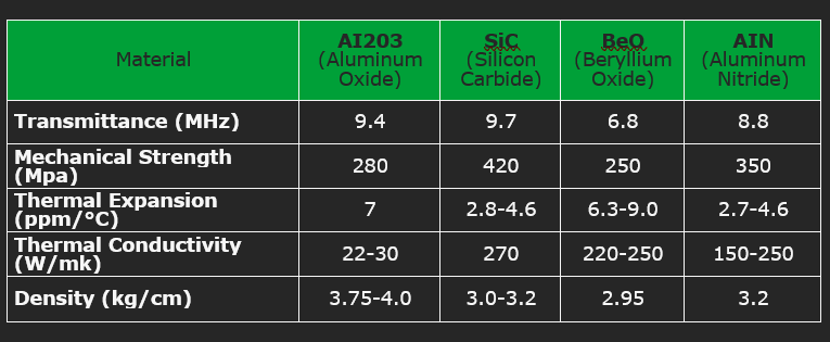
If you are designing your PCBs for use under high pressure, high insulation, high frequency, high temperature, high reliability and small volume products, Ceramic PCB will be the best choice for you. They are the boards with very high thermal conductivity and very low coefficient of expansion (CTE). Ceramic PCB boards are made of ceramic materials such as aluminum nitride, aluminum oxide, beryllium oxide and silicon carbide. Aluminum nitride and beryllium oxide give the best performance, but aluminum oxide may be preferred when the budget is tight. The conductivity of aluminum nitride circuit boards ranges from 150-250 W/mK, while the conductivity of aluminum oxide is 22-30 W/mK. It will ensure efficient and effective operation of your device at temperatures up to 350°C, eliminating the risk of deterioration unlike other PCB materials exposed to high temperatures. Ceramic PCBs play a vital role in the development of miniature electronic products. (CTE represents the coefficient of thermal expansion, which refers to the expansion of materials due to heat.)
Types of Ceramic PCBs;
Thick Film Ceramic;
It corresponds to the thickness of the gold and conductive layer applied on a ceramic base material. Thick film ceramic sheets have a conductive layer exceeding 10 microns (10~13um). The PCB thickness may be less than FR4 or DCB board. Baking temperatures of up to 1000°C can be used in manufacturing.
The biggest benefit of thick film ceramic material compared to traditional PCBs is that thick film ceramics prevent oxidation of copper. Therefore, thick film ceramic circuits should be preferred when there is a concern about oxidization of the boards.
Some areas of use;
● High power LEDs
● Street lights, high bright lights
● Automotive light systems
● Hybrid integrated circuits for automotive
● Fuel sender resistance boards
● Injection systems
● Solar cells
Thin Film Ceramic PCB;
The thickness of the conductive layer on the ceramic PCB is less than 10 microns. Compared with thick film ceramic PCBs, the main elements of thin film circuits are of smaller size. However, the manufacturing equipment used is more expensive, and the manufacturing cost is higher. During the manufacturing process, several ways of manufacturing thin film layers are preferred, such as physical vapor deposition (PVD), which is popular, and anodic oxidation or electroplating as a less popular option. Thin film Ceramic PCB is suitable for a variety of circuits, especially for analog ones, which require high accuracy, excellent stability and excellent performance. It is usually used in microwave circuits.
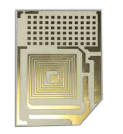
DCB Ceramic PCB;
These are circuit boards in which aluminum nitride or aluminum oxide is directly connected with copper foil under high temperature. It is also known as DBC (Direct Bond Copper) technology. This technique offers electrical insulation, high thermal conductivity, fine solderability and high adhesion strength. It has high current loading capacities and can be copper-etched like normal FR4 PCBs.
Advantages of Ceramic PCB:
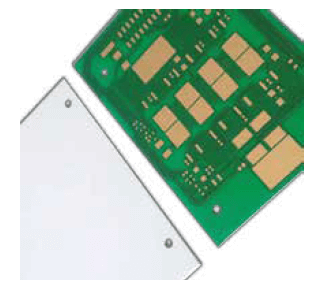
The most widely used and preferred PCB material is FR4 material. However, one of the main reasons for using Ceramic PCB instead of FR4 is that the heat transfer is better. Other advantages:
● The soldering quality of the substrate is good, and the temperature of use is high.
● High temperature resistance and high electrical insulation performance,
● Good chemical stability and low frequency loss,
● Organic component-free, cosmic ray resistant and long-lasting use,
● The copper layer does not contain an oxide layer and can be used for a long time in a reducing atmosphere.
● Can be installed with high density.
Disadvantages of Ceramic PCB;
Fragility
One of the difficulties of ceramic-based PCB is that it is fragile. This also affects the size of the PCB you can manufacture.
Cost
There are many processes in the manufacture of ceramic PCBs. In addition, it is used very rarely compared to PCB materials such as FR4, CEM1, ALU. This also makes them expensive
Use
Ceramic PCBs can be very complicated, as the material is fragile and small. Any issue related to the board can take huge effort and time to fix. Ceramic PCBs are very small as they are made for tight spaces, which makes it even more difficult to transport.
Areas of Use of Ceramic PCBs:
Ceramic PCBs are used for a wide range of high-performance PCBs used in aerospace, automotive, medical devices, heavy machinery, solar panel arrays, power transmitter module and solid-state relays. Other areas of use;
● Spotlights and high current LEDs
● Power controls
● Variable optical systems
● Power regulators for automobiles
● Industrial power equipment
● Semiconductor cooling devices
● Printers
● Sound amplifiers
● High-power transistors and transistor arrays